Implementing Manchester and BMC encoder/decoder on EFM8LB1
1. Introduction
The Manchester code and Biphase Mark Code(BMC) are popular line code which conveys the data and clock information. Here will introduce how to implement Manchester and BMC encoder/decoder on Silicon Labs EFM8LB1 with its Configurable Logic Units(CLU).
2. Manchester code
Manchester Code is widely used(e.G., In 10BASE-T Ethernet(IEEE802.3)). The encoding of each bit is either low then high, or high then low, of equal time. For IEEE802.3 standard, "1" is represented by a rising edge. "0" is represented by a failing edge. It has no DC component, and is self-clocking.
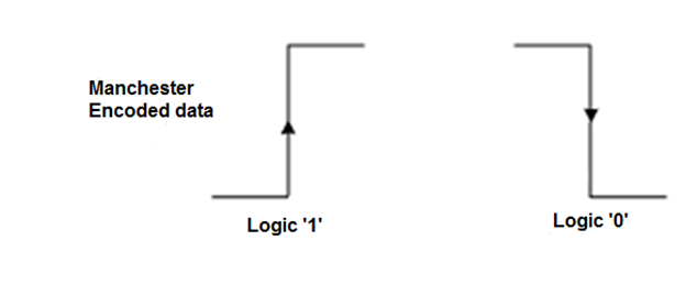
Figure 1 Manchester Bit Data (IEEE802.3)
2.1. Manchester Encoder
It is easy to generate Manchester encoded data by XOR SPI MOSI and SCK signals. The SCK phase and polarity setting (CKPOL = 0, CKPHA = 1). the EFM8LB1 CLU setting to implement Manchester Encoder as follows.
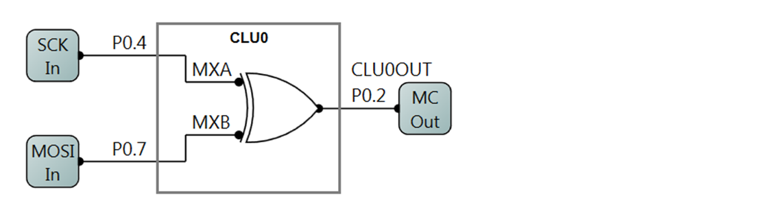
Figure 2 Manchester Encoder
The CLU configuration code as follows:
SFRPAGE = 0x20;
/* MXA as P0.4, MXB as P0.7*/
CLU0MX = 0xAB;
CLU0FN = LUT_XOR(SI_LUT_A, SI_LUT_B);
CLU0CF = CLU0CF_OEN__ENABLE |         CLU0CF_OUTSEL__LUT;
CLEN0 |= CLEN0_C0EN__ENABLE;
SFRPAGE = 0;
The Manchester Encoder waveform is shown as follows:
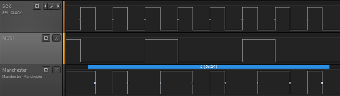
Figure 3 Manchester Encoder Waveform
From the waveform, when MOSI = 0, the XORed output follows SCK, it is failing edge = '0'; When MOSI = 1, the XORed output is an inverted SCK, it is rising edge = '1'.
2.2. Manchester Decoder
The Manchester bit value is presented in the second half of each bit time. Here we can generate a clock to capture the value at second half of bit time. The transition in middle of each bit triggers timer with 3/8 bit time. Generating SCK rising edge when timer overflow. Generating SCK failing edge when timer overflow again and stop the timer. Repeat above steps for rest bits.
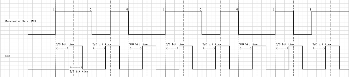
Figure 4 Manchester Decoder Clock Generation
How to trigger the Timer at Manchester middle transition? First, Generating latch data by capturing the data at 6/8 bit time. Second, Manchester data XOR latch data to get rising edge at middle transition. The XOR result at 6/8 bit must be ‘0’, because latch data captures same MC data. And then at middle transition, the XOR result change to ‘1” and generate rising edge. Now we got the rising edge of middle transition, this is can be used to trigger Timer with D flip-flop to start with 3/8 bit time.
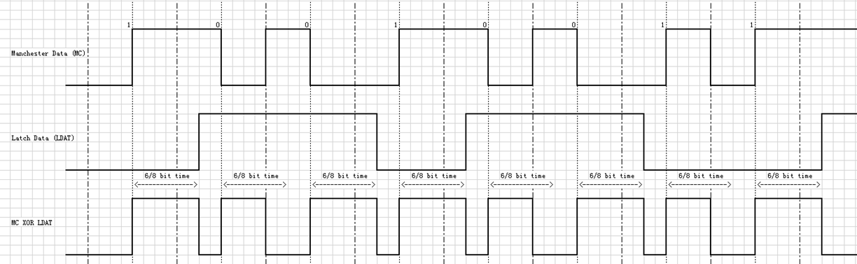
Figure 5 Manchester Decoder Clock Trigger Signal Generator
How to control Timer? The MC XOR LDAT rising edge start timer. Timer stops after 6/8 bit time. From the observation on the timing diagram, we can get Boolean Equation is F = A NOR B. Where the A represents MC XOR LDAT, B represents SCK. The F represents TMR2 Force reload signal.
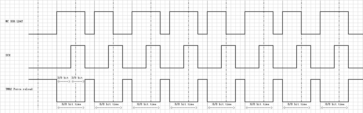
Figure 6 Manchester Decoder Timer Control
This is implementation of Manchester Decoder. It uses four CLUs. The CLU2 uses internal D flip-flop, MC as D input, output is Latch MC, Clock source is carry from CLU1. The CLU1 uses internal D flip-flop too, it generates clock signal, the D flip-flop clock source comes from Timer 2 overflow signal. CLU3 buffer MC data and output as carry signal of CLU0. the CLU0 combine three inputs MC, Latched MC and Clock to generate Timer2 force reload signal.
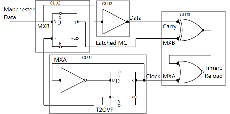
Figure 7 Manchester Decoder Implementation
CLU0MX = CLU0MX_MXA__CLU0A1 | CLU0MX_MXB__CLU0B2;
CLU0CF = CLU0CF_OUTSEL__LUT | CLU0CF_OEN__ENABLE;
CLU0FN = LUT_NOR(SI_LUT_A, LUT_XOR(SI_LUT_B, SI_LUT_C));

CLU1MX = CLU1MX_MXA__CLU1A1 | CLU1MX_MXB__CLU1B1;
CLU1CF = CLU1CF_OEN__ENABLE | CLU1CF_CLKSEL__ALTCLK;
CLU1FN = LUT_NOT(SI_LUT_A);

CLU2MX = CLU2MX_MXA__CLU2A0 | CLU2MX_MXB__CLU2B8;
CLU2CF = CLU2CF_CLKSEL__CARRY_IN | CLU2CF_OEN__ENABLE;
CLU2FN = SI_LUT_B;

CLU3MX = 0x00;
CLU3CF = CLU3CF_OUTSEL__LUT | CLU3CF_OEN__ENABLE;
CLU3FN = SI_LUT_C;

CLEN0   = 0x0F; // enable CLU0, CLU1, CLU2, CLU3
The overall view on all related signals of Manchester Decoder as follows.
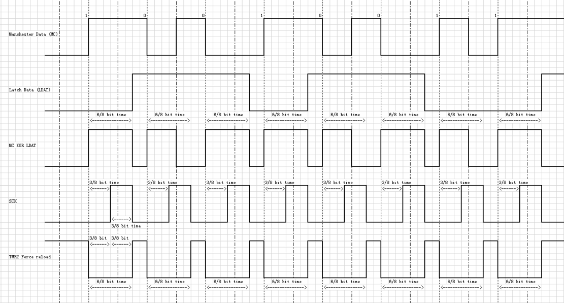
Figure 8 Manchester Decoder Waveform
3. Biphase Mark Code
Biphase Mark Code(BMC) uses the presence or absence of transitions to indicate logical value. BMC transitions on every positive edge of the clock signal BMC transitions on negative edge of the clock signal when the data is a 1.
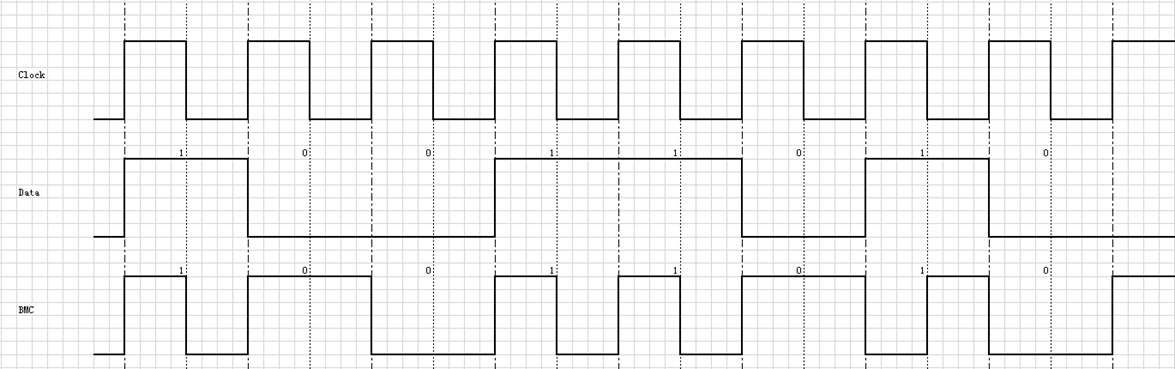
Figure 9 BMC Data
3.1. BMC Encoder
To encode the BMC data, first at all, generating transition for data 1. Here we choose a way to XOR Data and Q1, where Q1 is the D flip-flop output, and Q1 XOR Data as the input of D flip-flop. When data is 1, at first half bit time, the Q1 ^ Data = Not Q1. At the failing edge of clock, the Q1 captures the Not Q1, which generate a transition at middle bit time. When the data is 0, the Q1 keeps unchanged, no transition happens.
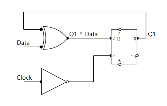
Figure 10 BMC Encoder Transitions on Data 1
And the waveform of transitions on data 1 is shown as follows:
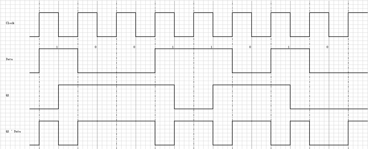
Figure 10 BMC Encoder Waveform of Transitions on Data 1
From the timing diagram, we can see the D flip-flop captures the Q1 XOR Data at failing edge of clock. For data = 1, there is a transition at the time, for data = 0, there is not transition at the time. And also we notice that Q1 keeps unchanged at the beginning of each bit, the D flip-flop maintains the Q value before the rising edge of the clock.
The second step, we need to generate transition at beginning of each bit. The idea here is that we flip first bit, and keeps second bit unchanged, and then flip third bit, and keep fourth bit unchanged, etc. So we use Q2 which is the clock by 2 and XOR the Q1 to generate BMC data. When Q2 is 1, the Q1 ^ 1 = Not Q1, it makes transition. When Q2 is 0, the Q1 ^ 0 = Q1, it changes nothing. And finally, we get BMC data with transitions at beginning of every bit. And also transition at middle bit when data is 1.

Figure 11 BMC Encoder Transitions at Beginning of Every Bit
Here is the implementation of the BMC Encoder. It uses four CLUs. For CLU0, it generates Q2 which is the clock divided by 2. For CLU1 and CLU3, they generate Q1 which contains transition at middle bit time when data is 1. The CLU2 XOR the Q1 and Q2, output the BMC encoding data.
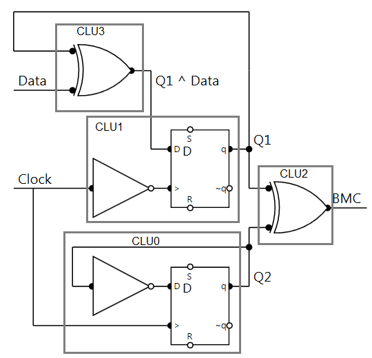
Figure 12 BMC Encoder Implementation
Here are all signals waveform we talked previously.
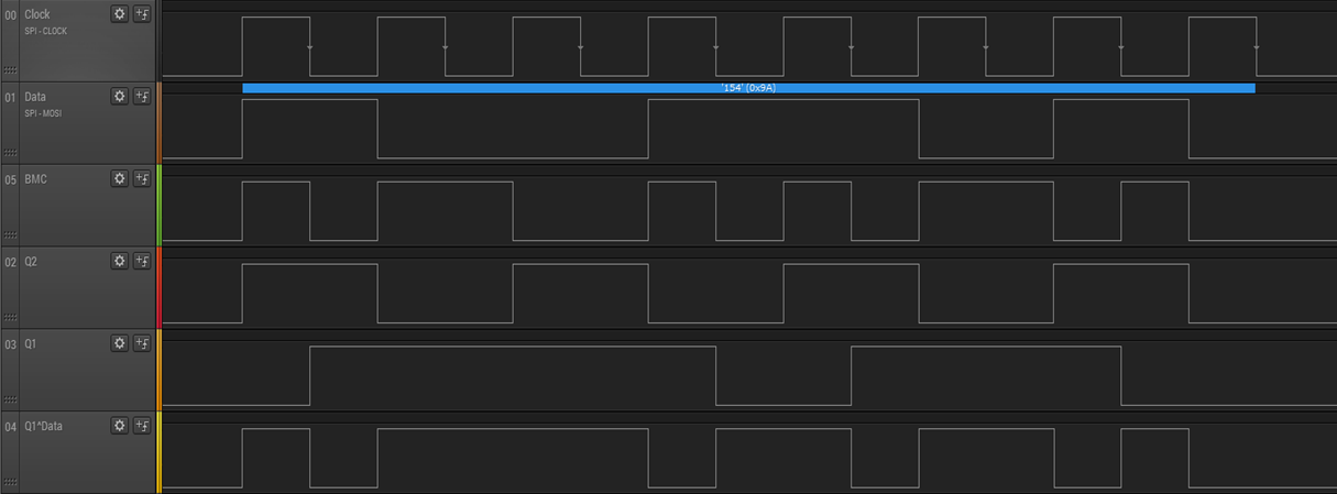
Figure 13 BMC Encoder Waveform
3.2. BMC Decoder
The BMC decoder needs more logical circuitry, base one the resource we have in one EFM8LB1 device, here we made a solution to decode the BMC data with minimums hardware resources we can. As we talked in previous slides. The BMC transition at beginning of each bit or middle or bit when data = 1. Here is the timing diagram of BMC, From the observation, we capture the data at 6/8 bit time. When the value between first sample point and second sample point is same, that means second bit is “1”. That is because the transition happens twice at bit boundary and middle of second bit. When the value between first sample point and second sample is difference, that means second b it is “0”. That is because the transition happens once, at bit boundary. Base on above analysis. We can use XNOR two sample points value to generate data which apart from 6/8 bit time compare with BMC data. And using a timer to generate SCK which rising edge at beginning of each bit.
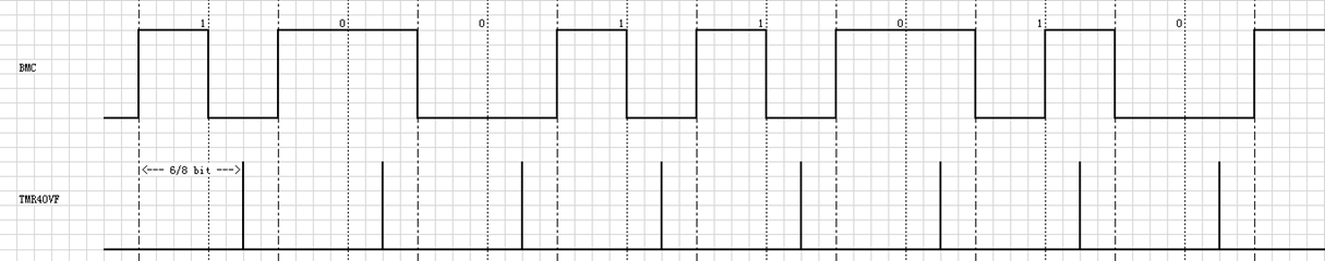
Figure 14 BMC Decoder Method
The Timer control is very important in BMC decoder design. The Timers are used to capture the data and generate clock. Here is the requirement on Timer setting, Timer starts from beginning of each bit, and Timer stops at 6/8 bit time. To achieve the functionality, we choose two signals to control Timer: Timer OVF signal, and BMC XNOR prior BMC 6/8 bit value. The Time OVF is low at beginning of the bit since it is stop. It can be used to start timer when BMC XNOR PBMC change to 0 at beginning of each bit. The XNOR result start from 6/8 bit time must be “1”, since it is same value after capturing data at that point. It can be use to stop timer.
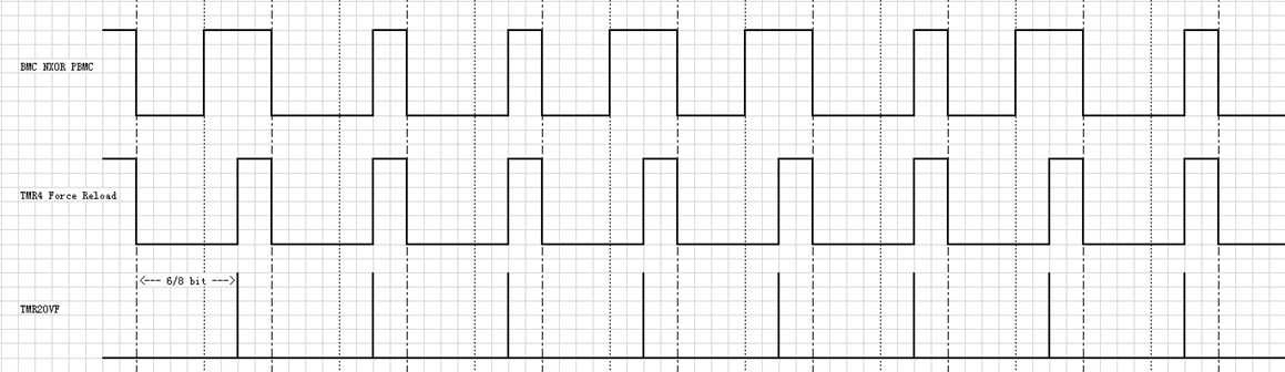
Figure 15 BMC Decoder Timer Control
Here is the timing diagram on clock and data generation. BMC data XNOR prior BMC value at 6/8 bit time to generate Data. And the Timer force reload signal can be inversed as clock. The SCK second edge to capture the data which is beginning of each bit of BMC data.
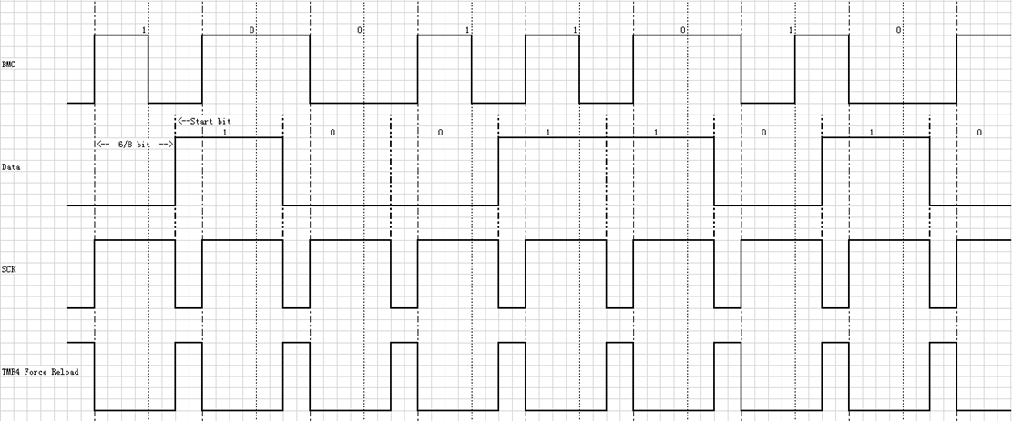
Figure 16 BMC Decoder Data and Clock Generation
Here is the CLU implementation for BMC decoder. The CLU0 act as a selector, the Boolean expression is BC + B’A. It selects T2OVF or Carry In which is XNOR result of BMC and PBMC, the T2OVF is one clock after T4OVF, which make sure when T2OVF is high, the selector captures the value from Carry in is high. That is because after 6/8 bit time, the XNOR result must be high, which stops the Timers. the CLU0 output is Timer Reload force. The CLU1 invert CLU0 output as Clock output. The CLU2 and CLU3 are combined together to generate Data. When T4OVF happens, it generates on system clock width pulse. At rising edge, the CLU3 captures the XNOR result and output as Data; at failing edge, the CLU2 captures 6/8 bit time BMC value. And the XNOR result as carry in signal to CLU0 to control the Timer start-stop.
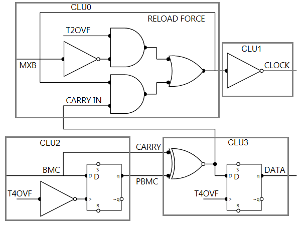
Figure 17 BMC Decoder Implementation
CLU0MX = 0x40; // MXA as T2OVF, MXB as CLU0 output
CLU0CF = CLU0CF_OUTSEL__LUT;
CLU0FN = LUT_OR(LUT_AND(SI_LUT_B, SI_LUT_C),
            LUT_AND(LUT_NOT(SI_LUT_B), SI_LUT_A));

CLU1MX = 0x00; // MXA as CLU0 output
CLU1CF = CLU1CF_OEN__ENABLE | CLU1CF_OUTSEL__LUT;
CLU1FN = LUT_NOT(SI_LUT_A);

CLU2MX = 0x48; // MXA as T4OVF, MXB as P0.2
CLU2CF = CLU2CF_CLKINV__INVERT | CLU2CF_CLKSEL__MXA_INPUT;
CLU2FN = SI_LUT_B;

CLU3MX = 0x22; // MXA as CLU2 output;
CLU3CF = CLU3CF_OEN__ENABLE | CLU3CF_CLKSEL__ALTCLK;
CLU3FN = LUT_XNOR(SI_LUT_A, SI_LUT_C);

CLEN0   = 0x0F; // enable CLU0, CLU1, CLU2, CLU3
Here are the BMC data, SPI SCK, MOSI signals waveform. We can see the data start from 6/8 bit time compare with BMC data. The MOSI data is valid on second edge of SCK period (PHA=1).
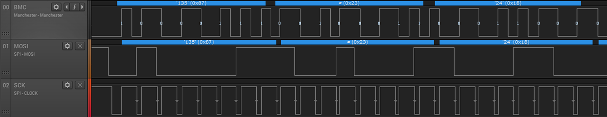
Figure 18 BMC Decoder Waveform
4. LICENSE
The MIT License (MIT)
Copyright (c) 2015 Mark Ding(mark.ding@hotmail.com)
Permission is hereby granted, free of charge, to any person obtaining a copy of this software and associated documentation files (the "Software"), to deal in the Software without restriction, including without limitation the rights to use, copy, modify, merge, publish, distribute, sub-license, and/or sell copies of the Software, and to permit persons to whom the Software is furnished to do so, subject to the following conditions:
The above copyright notice and this permission notice shall be included in all copies or substantial portions of the Software.
THE SOFTWARE IS PROVIDED "AS IS", WITHOUT WARRANTY OF ANY KIND, EXPRESS OR IMPLIED, INCLUDING BUT NOT LIMITED TO THE WARRANTIES OF MERCHANTABILITY, FITNESS FOR A PARTICULAR PURPOSE AND NONINFRINGEMENT. IN NO EVENT SHALL THE AUTHORS OR COPYRIGHT HOLDERS BE LIABLE FOR ANY CLAIM, DAMAGES OR OTHER LIABILITY, WHETHER IN AN ACTION OF CONTRACT, TORT OR OTHERWISE, ARISING FROM, OUT OF OR IN CONNECTION WITH THE SOFTWARE OR THE USE OR OTHER DEALINGS IN THE SOFTWARE.