Sep 6, 2017
Jlink Python Programming GUI Tool
1 Introduction
We use Python+Pyside make a GUI programming tool. By calling JLinkARM.Dll, it can access the device via C2 and SWD interface. The EFM8 and EFM32 which are C8051 and ARM cortex M0/M3/M4 core are in the latest Segger JLinkARM.dll support list. It can download hex file, and also binary file with offset setting.
https://markding.github.io/pyprogrammer/
Dec 25, 2015
Manchester and Biphase Mark Code Encoder/Decoder Implementation
Implementing Manchester and BMC encoder/decoder on EFM8LB1
1. Introduction
The Manchester code and Biphase Mark Code(BMC) are popular line code which conveys the data and clock information. Here will introduce how to implement Manchester and BMC encoder/decoder on Silicon Labs EFM8LB1 with its Configurable Logic Units(CLU).
2. Manchester code
Manchester Code is widely used(e.G., In 10BASE-T Ethernet(IEEE802.3)). The encoding of each bit is either low then high, or high then low, of equal time. For IEEE802.3 standard, "1" is represented by a rising edge. "0" is represented by a failing edge. It has no DC component, and is self-clocking.
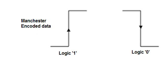
Figure 1 Manchester Bit Data (IEEE802.3)
2.1. Manchester Encoder
It is easy to generate Manchester encoded data by XOR SPI MOSI and SCK signals. The SCK phase and polarity setting (CKPOL = 0, CKPHA = 1). the EFM8LB1 CLU setting to implement Manchester Encoder as follows.
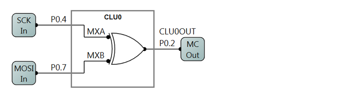
Figure 2 Manchester Encoder
The CLU configuration code as follows:
SFRPAGE = 0x20;
/* MXA as P0.4, MXB as P0.7*/
CLU0MX = 0xAB;
CLU0FN = LUT_XOR(SI_LUT_A, SI_LUT_B);
CLU0CF = CLU0CF_OEN__ENABLE |         CLU0CF_OUTSEL__LUT;
CLEN0 |= CLEN0_C0EN__ENABLE;
SFRPAGE = 0;
The Manchester Encoder waveform is shown as follows:
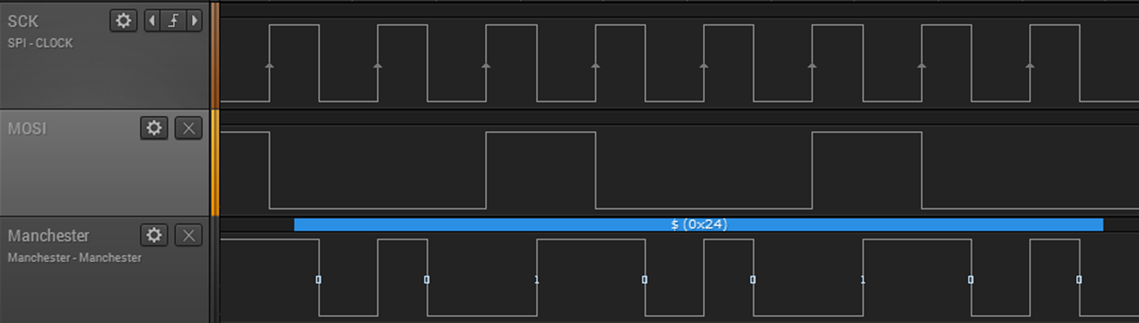
Figure 3 Manchester Encoder Waveform
From the waveform, when MOSI = 0, the XORed output follows SCK, it is failing edge = '0'; When MOSI = 1, the XORed output is an inverted SCK, it is rising edge = '1'.
2.2. Manchester Decoder
The Manchester bit value is presented in the second half of each bit time. Here we can generate a clock to capture the value at second half of bit time. The transition in middle of each bit triggers timer with 3/8 bit time. Generating SCK rising edge when timer overflow. Generating SCK failing edge when timer overflow again and stop the timer. Repeat above steps for rest bits.
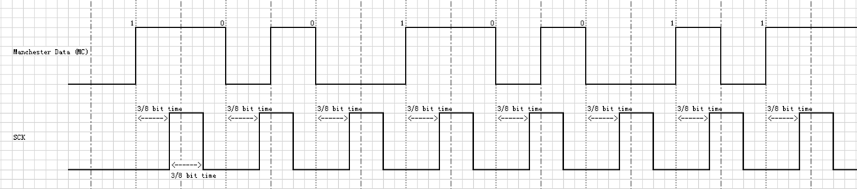
Figure 4 Manchester Decoder Clock Generation
How to trigger the Timer at Manchester middle transition? First, Generating latch data by capturing the data at 6/8 bit time. Second, Manchester data XOR latch data to get rising edge at middle transition. The XOR result at 6/8 bit must be ‘0’, because latch data captures same MC data. And then at middle transition, the XOR result change to ‘1” and generate rising edge. Now we got the rising edge of middle transition, this is can be used to trigger Timer with D flip-flop to start with 3/8 bit time.
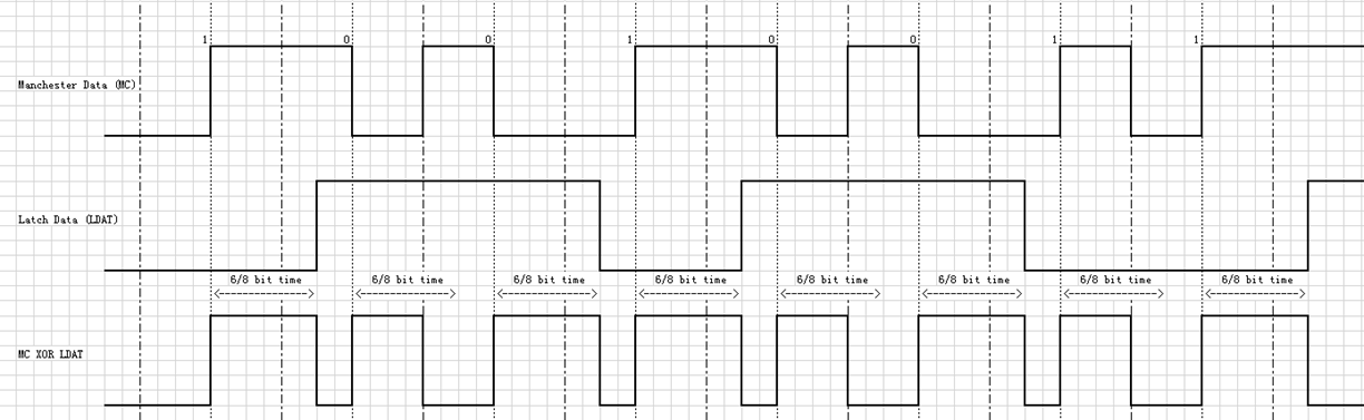
Figure 5 Manchester Decoder Clock Trigger Signal Generator
How to control Timer? The MC XOR LDAT rising edge start timer. Timer stops after 6/8 bit time. From the observation on the timing diagram, we can get Boolean Equation is F = A NOR B. Where the A represents MC XOR LDAT, B represents SCK. The F represents TMR2 Force reload signal.
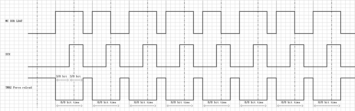
Figure 6 Manchester Decoder Timer Control
This is implementation of Manchester Decoder. It uses four CLUs. The CLU2 uses internal D flip-flop, MC as D input, output is Latch MC, Clock source is carry from CLU1. The CLU1 uses internal D flip-flop too, it generates clock signal, the D flip-flop clock source comes from Timer 2 overflow signal. CLU3 buffer MC data and output as carry signal of CLU0. the CLU0 combine three inputs MC, Latched MC and Clock to generate Timer2 force reload signal.
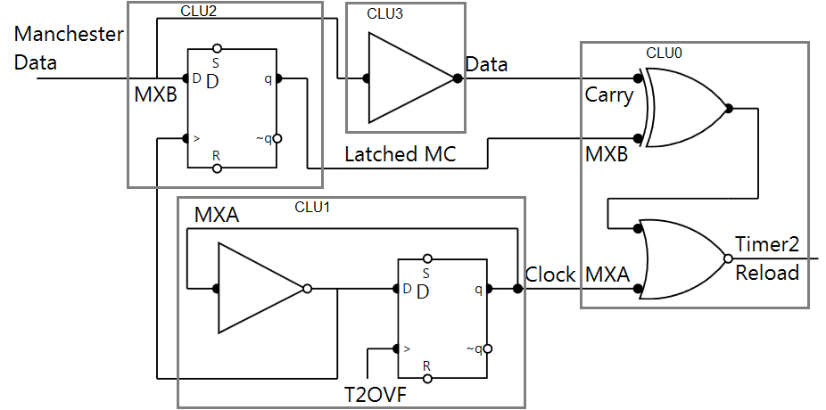
Figure 7 Manchester Decoder Implementation
CLU0MX = CLU0MX_MXA__CLU0A1 | CLU0MX_MXB__CLU0B2;
CLU0CF = CLU0CF_OUTSEL__LUT | CLU0CF_OEN__ENABLE;
CLU0FN = LUT_NOR(SI_LUT_A, LUT_XOR(SI_LUT_B, SI_LUT_C));

CLU1MX = CLU1MX_MXA__CLU1A1 | CLU1MX_MXB__CLU1B1;
CLU1CF = CLU1CF_OEN__ENABLE | CLU1CF_CLKSEL__ALTCLK;
CLU1FN = LUT_NOT(SI_LUT_A);

CLU2MX = CLU2MX_MXA__CLU2A0 | CLU2MX_MXB__CLU2B8;
CLU2CF = CLU2CF_CLKSEL__CARRY_IN | CLU2CF_OEN__ENABLE;
CLU2FN = SI_LUT_B;

CLU3MX = 0x00;
CLU3CF = CLU3CF_OUTSEL__LUT | CLU3CF_OEN__ENABLE;
CLU3FN = SI_LUT_C;

CLEN0   = 0x0F; // enable CLU0, CLU1, CLU2, CLU3
The overall view on all related signals of Manchester Decoder as follows.
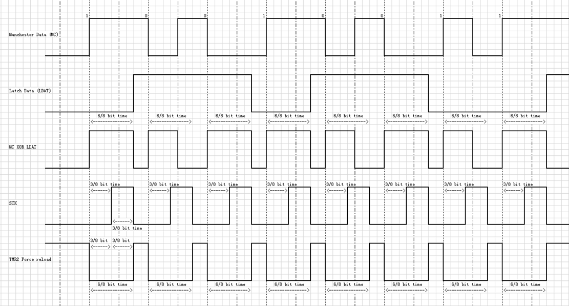
Figure 8 Manchester Decoder Waveform
3. Biphase Mark Code
Biphase Mark Code(BMC) uses the presence or absence of transitions to indicate logical value. BMC transitions on every positive edge of the clock signal BMC transitions on negative edge of the clock signal when the data is a 1.

Figure 9 BMC Data
3.1. BMC Encoder
To encode the BMC data, first at all, generating transition for data 1. Here we choose a way to XOR Data and Q1, where Q1 is the D flip-flop output, and Q1 XOR Data as the input of D flip-flop. When data is 1, at first half bit time, the Q1 ^ Data = Not Q1. At the failing edge of clock, the Q1 captures the Not Q1, which generate a transition at middle bit time. When the data is 0, the Q1 keeps unchanged, no transition happens.
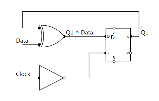
Figure 10 BMC Encoder Transitions on Data 1
And the waveform of transitions on data 1 is shown as follows:

Figure 10 BMC Encoder Waveform of Transitions on Data 1
From the timing diagram, we can see the D flip-flop captures the Q1 XOR Data at failing edge of clock. For data = 1, there is a transition at the time, for data = 0, there is not transition at the time. And also we notice that Q1 keeps unchanged at the beginning of each bit, the D flip-flop maintains the Q value before the rising edge of the clock.
The second step, we need to generate transition at beginning of each bit. The idea here is that we flip first bit, and keeps second bit unchanged, and then flip third bit, and keep fourth bit unchanged, etc. So we use Q2 which is the clock by 2 and XOR the Q1 to generate BMC data. When Q2 is 1, the Q1 ^ 1 = Not Q1, it makes transition. When Q2 is 0, the Q1 ^ 0 = Q1, it changes nothing. And finally, we get BMC data with transitions at beginning of every bit. And also transition at middle bit when data is 1.

Figure 11 BMC Encoder Transitions at Beginning of Every Bit
Here is the implementation of the BMC Encoder. It uses four CLUs. For CLU0, it generates Q2 which is the clock divided by 2. For CLU1 and CLU3, they generate Q1 which contains transition at middle bit time when data is 1. The CLU2 XOR the Q1 and Q2, output the BMC encoding data.
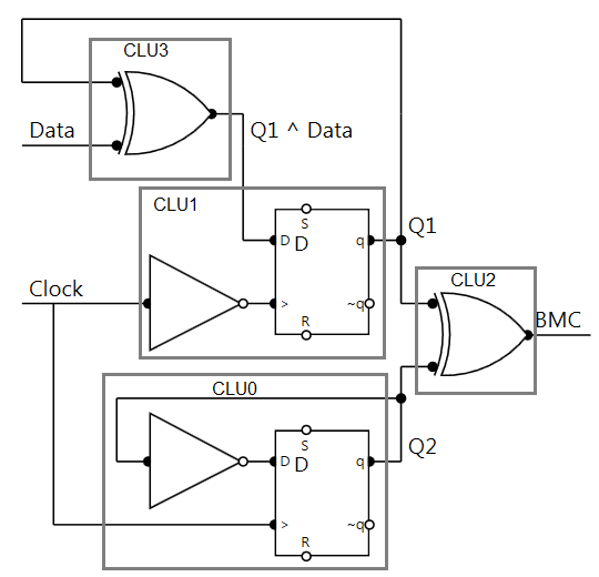
Figure 12 BMC Encoder Implementation
Here are all signals waveform we talked previously.

Figure 13 BMC Encoder Waveform
3.2. BMC Decoder
The BMC decoder needs more logical circuitry, base one the resource we have in one EFM8LB1 device, here we made a solution to decode the BMC data with minimums hardware resources we can. As we talked in previous slides. The BMC transition at beginning of each bit or middle or bit when data = 1. Here is the timing diagram of BMC, From the observation, we capture the data at 6/8 bit time. When the value between first sample point and second sample point is same, that means second bit is “1”. That is because the transition happens twice at bit boundary and middle of second bit. When the value between first sample point and second sample is difference, that means second b it is “0”. That is because the transition happens once, at bit boundary. Base on above analysis. We can use XNOR two sample points value to generate data which apart from 6/8 bit time compare with BMC data. And using a timer to generate SCK which rising edge at beginning of each bit.
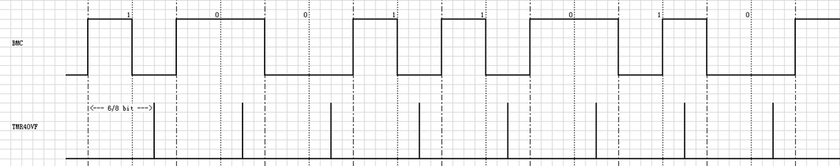
Figure 14 BMC Decoder Method
The Timer control is very important in BMC decoder design. The Timers are used to capture the data and generate clock. Here is the requirement on Timer setting, Timer starts from beginning of each bit, and Timer stops at 6/8 bit time. To achieve the functionality, we choose two signals to control Timer: Timer OVF signal, and BMC XNOR prior BMC 6/8 bit value. The Time OVF is low at beginning of the bit since it is stop. It can be used to start timer when BMC XNOR PBMC change to 0 at beginning of each bit. The XNOR result start from 6/8 bit time must be “1”, since it is same value after capturing data at that point. It can be use to stop timer.
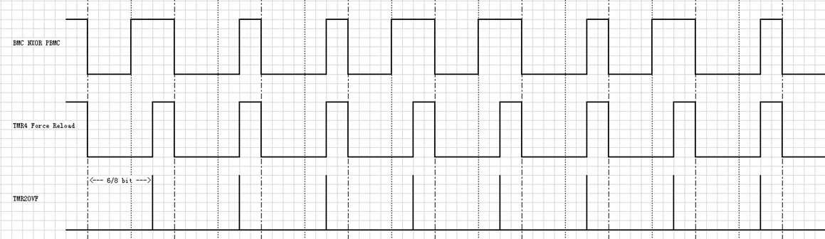
Figure 15 BMC Decoder Timer Control
Here is the timing diagram on clock and data generation. BMC data XNOR prior BMC value at 6/8 bit time to generate Data. And the Timer force reload signal can be inversed as clock. The SCK second edge to capture the data which is beginning of each bit of BMC data.
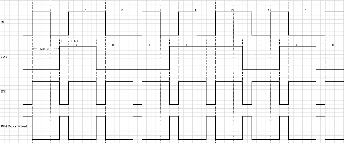
Figure 16 BMC Decoder Data and Clock Generation
Here is the CLU implementation for BMC decoder. The CLU0 act as a selector, the Boolean expression is BC + B’A. It selects T2OVF or Carry In which is XNOR result of BMC and PBMC, the T2OVF is one clock after T4OVF, which make sure when T2OVF is high, the selector captures the value from Carry in is high. That is because after 6/8 bit time, the XNOR result must be high, which stops the Timers. the CLU0 output is Timer Reload force. The CLU1 invert CLU0 output as Clock output. The CLU2 and CLU3 are combined together to generate Data. When T4OVF happens, it generates on system clock width pulse. At rising edge, the CLU3 captures the XNOR result and output as Data; at failing edge, the CLU2 captures 6/8 bit time BMC value. And the XNOR result as carry in signal to CLU0 to control the Timer start-stop.
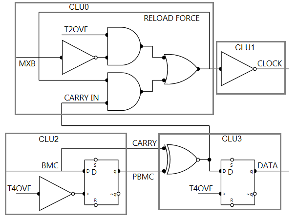
Figure 17 BMC Decoder Implementation
CLU0MX = 0x40; // MXA as T2OVF, MXB as CLU0 output
CLU0CF = CLU0CF_OUTSEL__LUT;
CLU0FN = LUT_OR(LUT_AND(SI_LUT_B, SI_LUT_C),
            LUT_AND(LUT_NOT(SI_LUT_B), SI_LUT_A));

CLU1MX = 0x00; // MXA as CLU0 output
CLU1CF = CLU1CF_OEN__ENABLE | CLU1CF_OUTSEL__LUT;
CLU1FN = LUT_NOT(SI_LUT_A);

CLU2MX = 0x48; // MXA as T4OVF, MXB as P0.2
CLU2CF = CLU2CF_CLKINV__INVERT | CLU2CF_CLKSEL__MXA_INPUT;
CLU2FN = SI_LUT_B;

CLU3MX = 0x22; // MXA as CLU2 output;
CLU3CF = CLU3CF_OEN__ENABLE | CLU3CF_CLKSEL__ALTCLK;
CLU3FN = LUT_XNOR(SI_LUT_A, SI_LUT_C);

CLEN0   = 0x0F; // enable CLU0, CLU1, CLU2, CLU3
Here are the BMC data, SPI SCK, MOSI signals waveform. We can see the data start from 6/8 bit time compare with BMC data. The MOSI data is valid on second edge of SCK period (PHA=1).
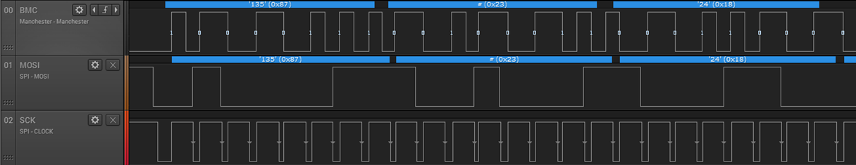
Figure 18 BMC Decoder Waveform
4. LICENSE
The MIT License (MIT)
Copyright (c) 2015 Mark Ding(mark.ding@hotmail.com)
Permission is hereby granted, free of charge, to any person obtaining a copy of this software and associated documentation files (the "Software"), to deal in the Software without restriction, including without limitation the rights to use, copy, modify, merge, publish, distribute, sub-license, and/or sell copies of the Software, and to permit persons to whom the Software is furnished to do so, subject to the following conditions:
The above copyright notice and this permission notice shall be included in all copies or substantial portions of the Software.
THE SOFTWARE IS PROVIDED "AS IS", WITHOUT WARRANTY OF ANY KIND, EXPRESS OR IMPLIED, INCLUDING BUT NOT LIMITED TO THE WARRANTIES OF MERCHANTABILITY, FITNESS FOR A PARTICULAR PURPOSE AND NONINFRINGEMENT. IN NO EVENT SHALL THE AUTHORS OR COPYRIGHT HOLDERS BE LIABLE FOR ANY CLAIM, DAMAGES OR OTHER LIABILITY, WHETHER IN AN ACTION OF CONTRACT, TORT OR OTHERWISE, ARISING FROM, OUT OF OR IN CONNECTION WITH THE SOFTWARE OR THE USE OR OTHER DEALINGS IN THE SOFTWARE.
Apr 7, 2015
Using pyvisa to control instrument via GPIB
1. Introduction
We have met several issues which related with power on/off operation. The failure rate is extremely low which is not efficiency for manual operation. So we would like to setup an automatic testing environment. The GPIB(General Purpose Interface Bus) is the way to control the instrument. This article shows how to control the Agilent E3631A (Triple Output DC Power Supply).
2. GPIB Interface
Here is the Agilent 82357A USB/GPIB Interface in our hand. Following link shows the detailed information.
http://www.keysight.com/en/pd-1000004416%3Aepsg%3Apro-pn-82357A/usb-gpib-interface?cc=US&lc=eng
http://www.keysight.com/en/pd-1000004416%3Aepsg%3Apro-pn-82357A/usb-gpib-interface?cc=US&lc=eng
3. Pyvisa installation
Pyvisa is a Python package for support of the “Virtual Instrument Software Architecture” (VISA), in order to control measurement devices and test equipment via GPIB, RS232, Ethernet or USB.
To install the pyvisa by using pip:
$ pip install pyvisa
To install the pyvisa by using pip:
$ pip install pyvisa
Detailed information can be found in https://github.com/hgrecco/pyvisa
4. NI driver installation
Pyvisa has been tested with NI-VISA 3.2, which needs us to install its driver.
Download and install NIVISA541full.exe from following link http://www.ni.com/download/ni-visa-5.4.1/4626/en/
Download and install NIVISA541full.exe from following link http://www.ni.com/download/ni-visa-5.4.1/4626/en/
5. Agilent driver installation.
The GPIB interface is Agilent product, which needs its driver installed.
Download and install the latest IOLibSuite_17_0_19013.exe from following link.
http://www.keysight.com/main/software.jspx?ckey=1184883&lc=chi&cc=CN&nid=-34027.536881832&id=1184883
Download and install the latest IOLibSuite_17_0_19013.exe from following link.
http://www.keysight.com/main/software.jspx?ckey=1184883&lc=chi&cc=CN&nid=-34027.536881832&id=1184883
6. Using HP Agilent 82357A/82357B GPIB in NI
http://digital.ni.com/public.nsf/allkb/F7C187DBF09EBE1186256F550065BD32
In order to use the NI VISA drivers and both the HP Agilent and NI GPIB devices, you will need to enable:
In order to use the NI VISA drivers and both the HP Agilent and NI GPIB devices, you will need to enable:
- NIVISATulip.dll
- NI 488.2 from within the Agilent libraries
Complete the steps in the following document to enable NIVISATulip.dll:
KnowledgeBase 20KG1C7Z: Can I Use Both National Instruments (GPIB) and Agilent/HP (HPIB) Controllers in the Same System? (http://digital.ni.com/public.nsf/websearch/3B3626D9C1F999218625694200791AD7?OpenDocument)
KnowledgeBase 20KG1C7Z: Can I Use Both National Instruments (GPIB) and Agilent/HP (HPIB) Controllers in the Same System? (http://digital.ni.com/public.nsf/websearch/3B3626D9C1F999218625694200791AD7?OpenDocument)
Complete the following steps to enable NI 488.2 from within Agilent Connection Expert 15.x and 16.x:
- Select Tools»Agilent 488 from the pulldown menu.
- Select the Agilent 488 Options tab.
- Check Enable Agilent GPIB cards for 488 programs.
7. Agilent E3631A spec download
Download spec from http://www.keysight.com/main/techSupport.jspx?cc=CN&lc=chi&nid=-35721.384004.08&pid=836433&pageMode=OV
Here is part of the command list:
APPLy {P6V|P25V|N25V}[,{|DEF|MIN|MAX}[,{ |DEF|MIN|MAX}]]
    APPLy? [{P6V|P25V|N25V}]
OUTPut
    [:STATe] {OFF|ON}
    [:STATe]?
    :TRACk[:STATe] {OFF|ON}
    :TRACk[:STATe]?
8. Pyvisa tutorial
From pyvisa official website, we can find the tutorial https://pyvisa.readthedocs.org/en/master/tutorial.html.
Here is the example code to control E3631A output.
import visa

rm = visa.ResourceManager()
res = rm.list_resources()
print("Find following resources: ")
print(res)
print("Opening " + res[-1])

inst = rm.open_resource(res[-1])

# When sending command to E3631A, The "Rmt" and "Adrs" icon are on on the display
# panel. All input from panel are inactived, util you press "Store/Local" button.

inst.query("*IDN?")

inst.write("INST P6V") # Select +6V output
inst.write("VOLT 2.0") # Set output voltage to 3.0 V
inst.write("CURR 1.0") # Set output current to 1.0 A

# The APPLy command provides the most straightforward method to program the
# power supply over the remote interface.
#  inst.write("APPL P6V, 3.0, 1.0")


# power on/off
inst.write("OUTP OFF")
inst.write("OUTP ON")
Dec 25, 2014
efm32 an0060 encrypt aes128 support
In AN0060, there is a encrypt.exe which support AES256 only. But for ZG device supports AES128, we need to make a change and generate new exe file. The steps as follows:
- Download libtom source code
Goto https://github.com/libtom/libtomcrypt, get latest version 1.17. - Extract it and generate directory “libtomcrypt-1.17”
- Run msys under windows.
Here we use the msys from Railsinstaller directory
$ C:\RailsInstaller\DevKit\msys.bat
- In msys window, enter libtomcrypt-1.17, edit makefile.
Uncomment line 12 and 13, save and close it.
CC=gcc
LD=ld
- Generate libtomcrypt.a file
$ make
The generated lib file in “libtomcrypt-1.17” directory.
- Copy AN0060 encrypt.c into “libtomcrypt-1.17” directory.
The file can be found in C:\SiliconLabs\SimplicityStudio\v2\developer\sdks\efm32\v2\an\an0060_efm32_aes_bootloader\src\encrypt\encrypt.c - Modify encrypt.c to support AES128, save and close it.
On line 51 change the AES_KEY_SIZE from 32 to 16
-#define AES_KEY_SIZE 32
+#define AES_KEY_SIZE 16
- Generate encrypt.exe
$ gcc -o encrypt encrypt.c -I./src/headers -L./ -ltomcrypt
The generated encrypt.exe in “libtomcrypt-1.17” directory.
http://markding.github.io/2014/12/25/efm32-an0060-encrypt-aes128-support.html
Jun 24, 2014
Implementing USB communication device class (CDC) on EFM32GG MCUs
1. Introduction
USB revolutionized the PC peripheral space by making a very simple plug-and-play interface for users. As a result, many modern computers no longer support RS-232 serial COM ports, opting for the slimmer USB alternative. This can be an issue for the developer who needs a COM port for communication between a peripheral and host PC. A subset of the USB Communication DeviceClass (CDC) can be used to emulate a serial port providing a virtual COM port UART interface. This allows developers to use legacy applications with new products using the same COM port interface as before, with few hardware and software modifications.

Figure 1 USB CDC Virtual COM Port System
This application note describes the USB communications device class driver (or USB CDC) in detail and includes an implementation example for the Silicon Labs EFM32 Giant Gecko MCU.
1.1. Assumptions
This document assumes the following:
- A working knowledge of the C programming language.
- Familiarity with the USB 2.0 specification and terms and abbreviations defined by the USB specification.
- Familiarity with Silicon Labs EFM32GG development environment.
1.2. Features and Limitations
The CDC firmware implemented with this application note includes the following features:
- Emulates a serial COM port on PC that supports the CDC Abstract Control Model (ACM).
- Provides an abstract communication interface for data transfers between the host and the device.
- Handles standard Chapter 9 USB device requests.
- Handles CDC-specific requests from USB host.
- Notifies the USB host of status using an interrupt endpoint.
- Provides data communication with the USB host using a bulk endpoint.
- The following baud rates are supported: 600, 1200, 2400, 4800, 9600, 14400, 19200, 38400, 57600, 76800, 115200 and 230400 bps.
The example does not implement the following:
- No CTS/RTS control is performed, so flow control must be set to nonein the terminal program.
- RTS/DTR control is not implemented.
2. Relevant Documentation
EFM32 Giant Gecko Application Notes are listed on the following website: www.silabs.com/32bit-appnotes.
- AN758 IMPLEMENTING USB COMMUNICATION DEVICE CLASS (CDC) ON SiM3U1XX MCUs -- provides an implementation example on porting LUFA USB CDC on SiM3U1xx MCUs.
- AN0822 SIMPLICITY STUDIO USER’S GUIDE -- provides a description of the Simplicity Studio IDE features and environment.
- AN0065 EFM32 as USB Device -- provides a description of the EFM32 USB Device stack.
3. USB CDC Class
The USB communications device class (CDC) is a composite USB device class, and the class may include more than one interface. The CDC is used primarily for modems, but also for ISDN, fax machines, and telephony applications for performing regular voice calls. The Abstract Control Model subclass of CDC and bridges the gap between legacy modem devices and USB devices, enabling the use of application programs designed for older modems.
3.1. Class Requests
The class requests and class notifications supported are listed in Table 1.
Table 1. Abstract Control Model Requests
| Request | Code | Description |
|---|---|---|
| SET_LINE_CODING | 20h | Configures baud rate, stop-bits, parity, and numberof-character bits. |
| GET_LINE_CODING | 21h | Requests current DTE rate, stop-bits, parity, and number-of-character bits. |
| SET_CONTROL_LINE_STATE | 22h | RS232 signalused to tell the DCE device the DTE device is now present. |
These class-specific requests are used for device and call management.
3.1.1. Set Line Coding
This request allows the host to specify typical asynchronous line-character formatting properties.
| bmRequestType | bRequest | wValue | wIndex | wLength | Data |
|---|---|---|---|---|---|
| 00100001b | SET_LINE_CODING | 0 | interface | size of structure | line coding structure |
Table 2 defines the line coding properties.
Table 2. Line Coding Format
| Offset | Field | Size | Value | Description |
|---|---|---|---|---|
| 0 | dwDTERate | 4 | Number | Data terminal rate, in bits per second. |
| 4 | bCharFormat | 1 | Number | 0: 1 Stop bit 1: 1.5 Stop bits 2: 2 Stop bits |
| 5 | bParityType | 1 | Number | Parity: 0:None 1: Odd 2: Even 3: Mark 4: Space |
| 6 | bDataBits | 1 | Number | Data bits (5, 6, 7, 8 or 16). |
3.1.2. Get Line Coding
This request allows the host to find out the currently configured line coding. Table 2 defines the line coding properties.
| bmRequestType | bRequest | wValue | wIndex | wLength | Data |
|---|---|---|---|---|---|
| 10100001b | GET_LINE_CODING | 0 | interface | size of structure | line coding structure |
3.1.3. Set Control Line State
This request generates RS-232/V.24 style control signals. Table 3 defines control signal bitmap.
| bmRequestType | bRequest | wValue | wIndex | wLength | Data |
|---|---|---|---|---|---|
| 00100001b | SET_LINE_CONTROL_STATE | control signal bitmap | interface | 0 | none |
Table 3. Control Signal Bitmap
| Bit Position | Description |
|---|---|
| 15:2 | Reserved (Reset to zero). |
| 1 | Carrier control for half duplex modems. This signal corresponds to V.24 signal 105 and RS232 signal RTS. 0: Deactivate carrier. 1: Activate carrier. The device ignores the value of this bit when operating in full duplex mode. |
| 0 | Indicates to DCE if DTE is present or not.This signal corresponds to V.24 signal 108/2 and RS232 signal DTR. 0: DTE is not present. 1: DTE is present |
3.2. Class Notifictions
Table 4 shows the class notifications supported by the Abstract Control Model.
Table 4. Abstract Control Model Notifications
| Notification | Code | Description |
|---|---|---|
| SERIAL_STATE | 20h | Returns the current state of the carrier detects, DSR, break, and ring signal. |
Serial State
This notification sends an asynchronous message containing the current UART status.
| bmRequestType | bRequest | wValue | wIndex | wLength | Data |
|---|---|---|---|---|---|
| 10100001b | SERIAL_STATE | 0 | interface | 2 | UART state bitmap |
The data field for this notification is a bitmapped value that contains the current state of detects transmission carrier, break, ring signal, and device overrun error. These signals are typically found on a UART and are used for communication status reporting. A state is considered enabled if its respective bit is set to 1.
Note: The firmware example included with this application does not currently support state change
Table 5. UART State Bitmap
| Bit Position | Field | Description |
|---|---|---|
| 15:7 | Reserved (future use). | |
| 6 | bOverRun | Received data has been discarded due to overrun in the device. |
| 5 | bParity | A parity error occurred. |
| 4 | bFraming | A framing error occurred. |
| 3 | bRingSignal | State of ring signal detection of the device. |
| 2 | bBreak | State of break detection mechanism of the device. |
| 1 | bTxCarrier | State of transmission carrier. This signal corresponds to V.24 signal 106 and RS232 signal DSR. |
| 0 | bRxCarrier | State of receiver carrier detection mechanism of device. This signal corresponds to V.24 signal 109 and RS232 signal DCD |
3.3. Endpoint Configuration
Table 6 illustrates the endpoint configuration for the Abstract Control Model.
Table 6. UART State Bitmap
| Endpoint | Direction | Type | Max Packet Size | Description |
|---|---|---|---|---|
| EP0 | In/Out | Control | 64 | Standard requests, class requests. |
| EP1 | In | Interrupt | 16 | State notification from device to host. |
| EP2 | In | Bulk | 64 | Data transferfrom device to host. |
| EP3 | Out | Bulk | 64 | Data transfer from host to device. |
Figure 2 shows a standard CDC communication flow.

Figure 2. USB CDC Communication FLow
4. LUFA USB Stack
The USB CDC firmware example is based on the
LUFA open-source project. LUFA is an open-source complete USB stack released under the permissive MIT License. It includes support for many USB classes, both for USB Hosts and USB Devices. For USB Devices, the LUFA stack includes support for Audio Class, CDC Class, HID Class, Mass Storage Class, MIDI Class, and RNDIS Class. More information about the LUFA project can be found on the official website: http://www.fourwalledcubicle.com/LUFA.php- The USB CDC project contains a prebuilt LUFA USB stack documentation which locate at .\LUFA\Documentation\html. Double click on the index.html, the documentations shows in your default browser.

Figure 3. USB LUFA Libary Documentation
- This implementation support two boards of EFM32GG, STK3700 and DK3750. Default setting is DK3750, To change board selection, just modify macro definition in .\LUFA\Common\BoardTypes.h.
#if !defined(__DOXYGEN__)
    #define BOARD_                 BOARD_DK3750
    #if !defined(BOARD)
        #define BOARD              BOARD_DK3750
    #endif
#endif
For STK3700 board, there is no UART socket on board. UART signals are connected to EXP Header.

Figure 4. USART signals on STK3700 Expansion Header
5. USB CDC Driver
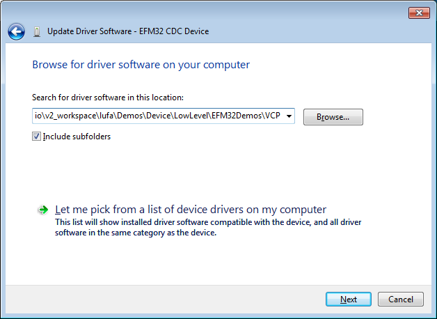
The CDC class is implemented in all releases of Windows, and the operatingsystem needs an INF file for the CDC driver. This INF file contains the Vendor ID and Product ID. If the VID/PID of the USB devices matches the INF file, Windows will load the driver described in the file. The VirtualSerial.inf file can be found in the.\Demos\Device\LowLevel\EFM32Demos\VCP directory.
Installing the Driver
To install the driver on Windows 7:
- Build the project and download firmware to the EFM32GG DK3750 board.
- Connect the USB cable between the Device MCU plugin board USB connector and the PC.
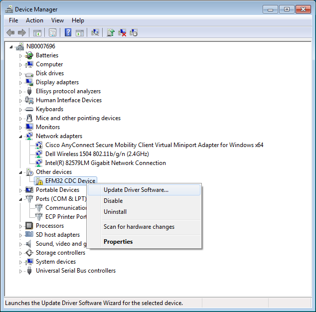
- Open Device Manager. The device will appear under Other devices as the EFM32GG CDC Device.
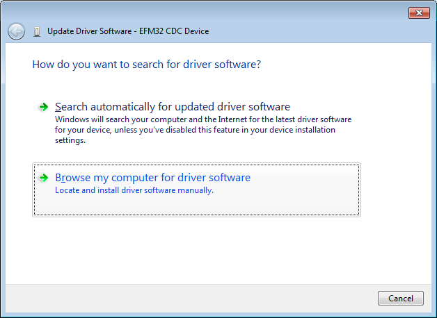
- Right-click on the EFM32GG CDC Device and select Update Driver Software.
- Select Browse my computer for driver software.
- Select Browse my computer for driver software.
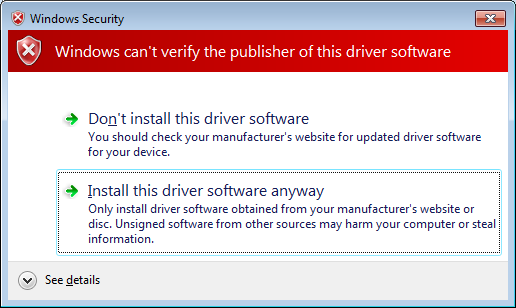
- Windows will display a warning. Select Install this driversoftware anyway.
- When the driver finishes installing,Windows will report the installation results.
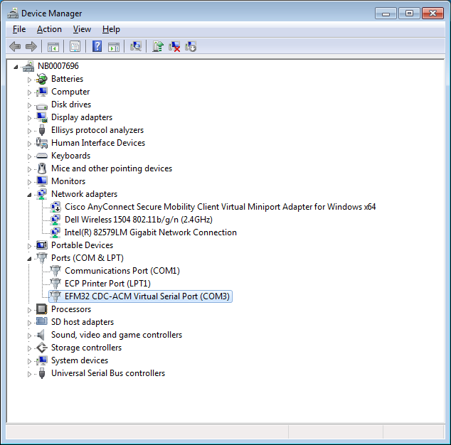
- Open Device Manager and observethe device. It will now appear under Ports (COM & LPT) with an assigned COM port number.

Source code
Source code can be found in https://github.com/MarkDing/lufa-efm32.
Github page in http://markding.github.io/lufa-efm32/.
CONTACT INFORMATION
Silicon Laboratories Inc. 400 West Cesar Chavez
Austin, TX 78701
Tel: 1+(512) 416-8500
Fax: 1+(512) 416-9669
Toll Free: 1+(877) 444-3032
Please visit the Silicon Labs Technical Support web page:
https://www.silabs.com/support/pages/contacttechnicalsupport.aspx
and register to submit a technical support request.
Austin, TX 78701
Tel: 1+(512) 416-8500
Fax: 1+(512) 416-9669
Toll Free: 1+(877) 444-3032
Please visit the Silicon Labs Technical Support web page:
https://www.silabs.com/support/pages/contacttechnicalsupport.aspx
and register to submit a technical support request.
Subscribe to:
Posts (Atom)